01
Laser head
Galvo-scanned laser. Etches, drills, routes, and cuts slots. No tool change.
Etch · drill · route · slot
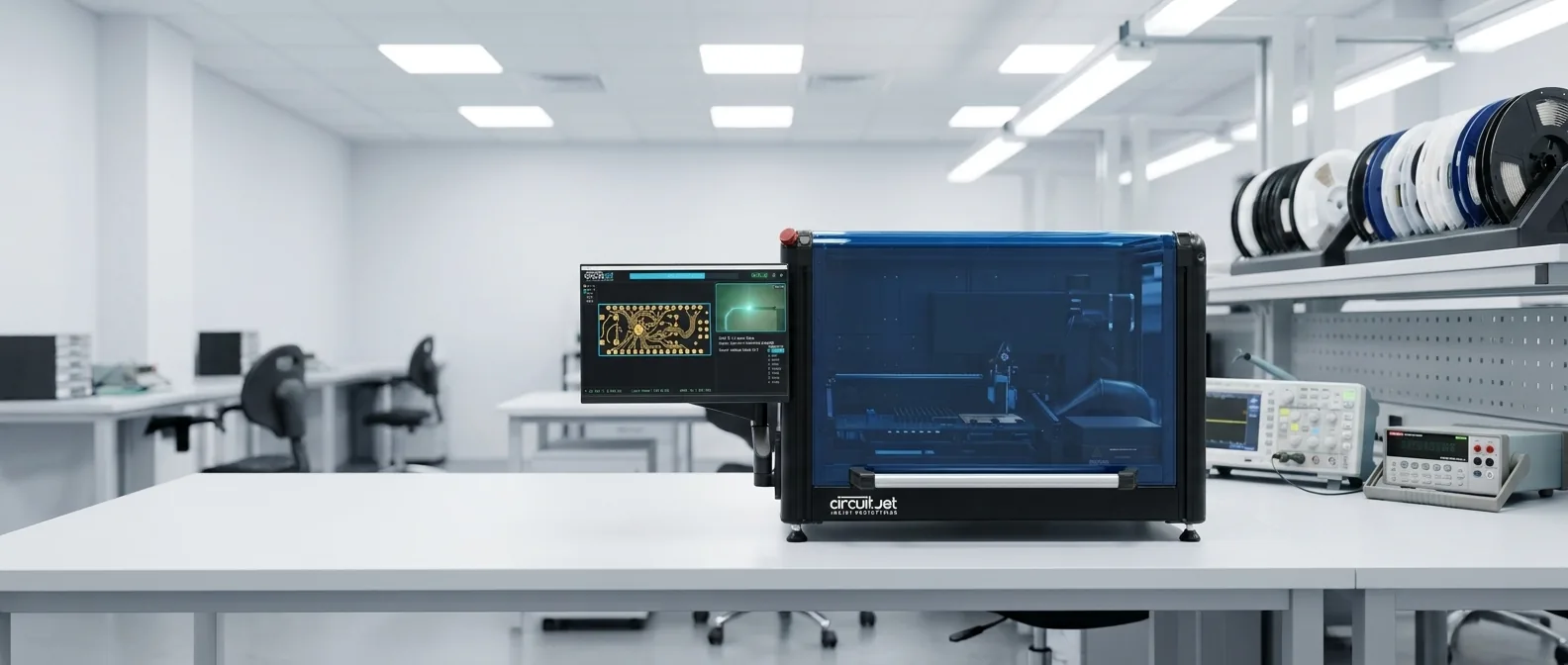
From bare copper-clad FR4 to populated board, in one machine. No chemical baths, no manual paste dispensing, no outsourced step.
The desktop PCBA foundry
The hard problem in rapid PCB prototyping has never been speed. It's been trust.
Electroninks has been a global leader in delivering advanced conductive inks to Tier 1 semiconductor and packaging manufacturers. CircuitJet IV is what happens when that materials expertise meets a benchtop laser, inkjet heads, a pick-and-place, and an AOI camera, all in one machine.
We start with raw copper. Standard FR4 copper-clad feedstock in. Bulk-copper traces out. Not conductive ink pretending to be a trace. Not chemically-milled copper swarf you bag and ship out. The traces are real copper because that's what you trust on a real product.
We use our materials only where they win. The hardest problem in desktop PCB fabrication has always been via plating, the step that turns two copper layers into a real two-layer circuit. Mill-based systems can't solve it without a chemical bath. We did, with our own novel inks: bath-free, inkjet-dispensed, fully conductive vias. No tanks. No chemistry. No outsourced step.
We don't hand you a half-built board. Pick-and-place and automated optical inspection are integrated. CircuitJet IV outputs a populated, inspected, 2-layer PCB in about two hours.
Standard substrates. Semiconductor-grade plating. Boards electrical designers won't scoff at.
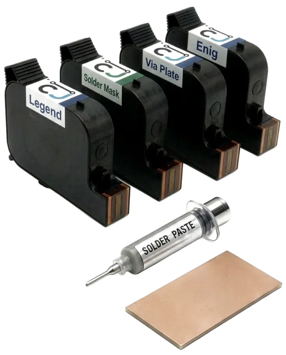
Four systems. One bench.
Galvo-scanned laser. Etches, drills, routes, and cuts slots. No tool change.
Etch · drill · route · slot
Solder mask, legend, and ENIG, each from its own dedicated cartridge. No tanks, no stencils, no screens.
Mask · Legend · ENIG
Single vacuum nozzle. Top and bottom vision. 0402 passives and standard SMT ICs.
0402 passives · Top + bottom vision
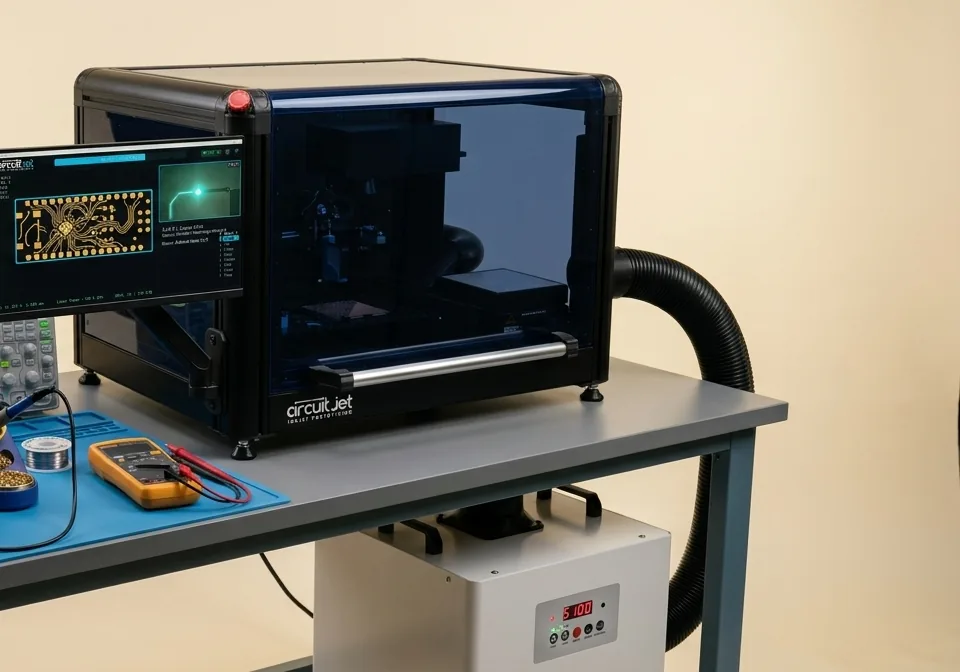
5-layer H13-grade HEPA filtration at 99.97%. Lets the machine run in any room, with no special ventilation required.
H13 HEPA · 99.97% · Office-safe
End-to-end run · Arduino Nano
Multiple processes, one fixture, all handled by the platform. The board never moves between machines. Laser, inkjet heads, pick-and-place, and AOI camera all reach the same workpiece without a re-registration step.
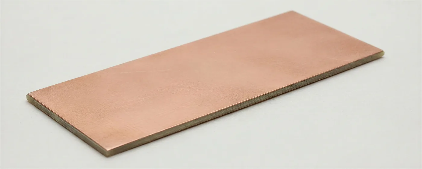
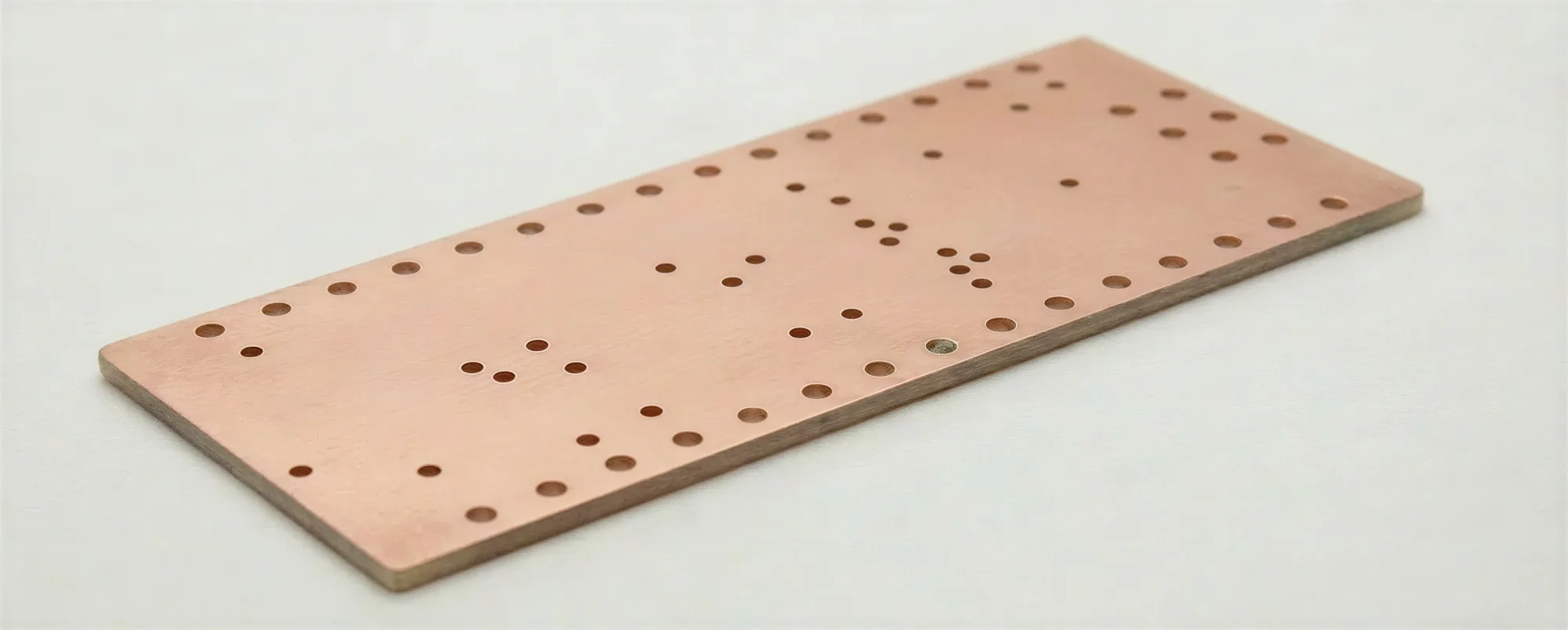
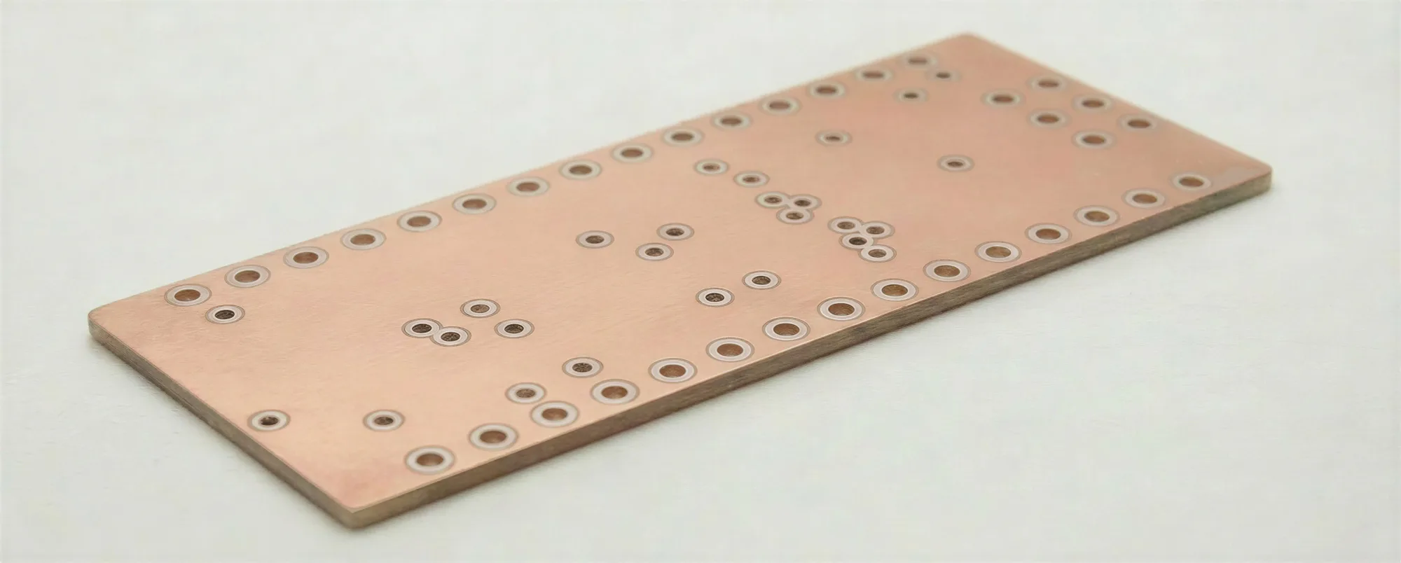
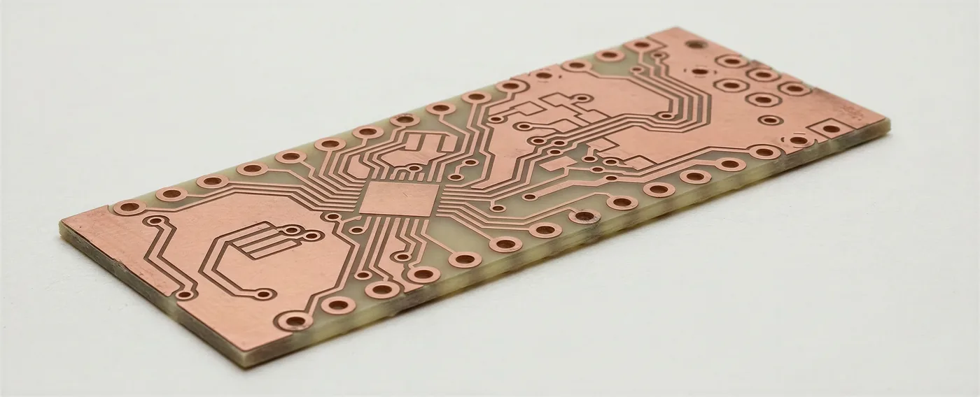
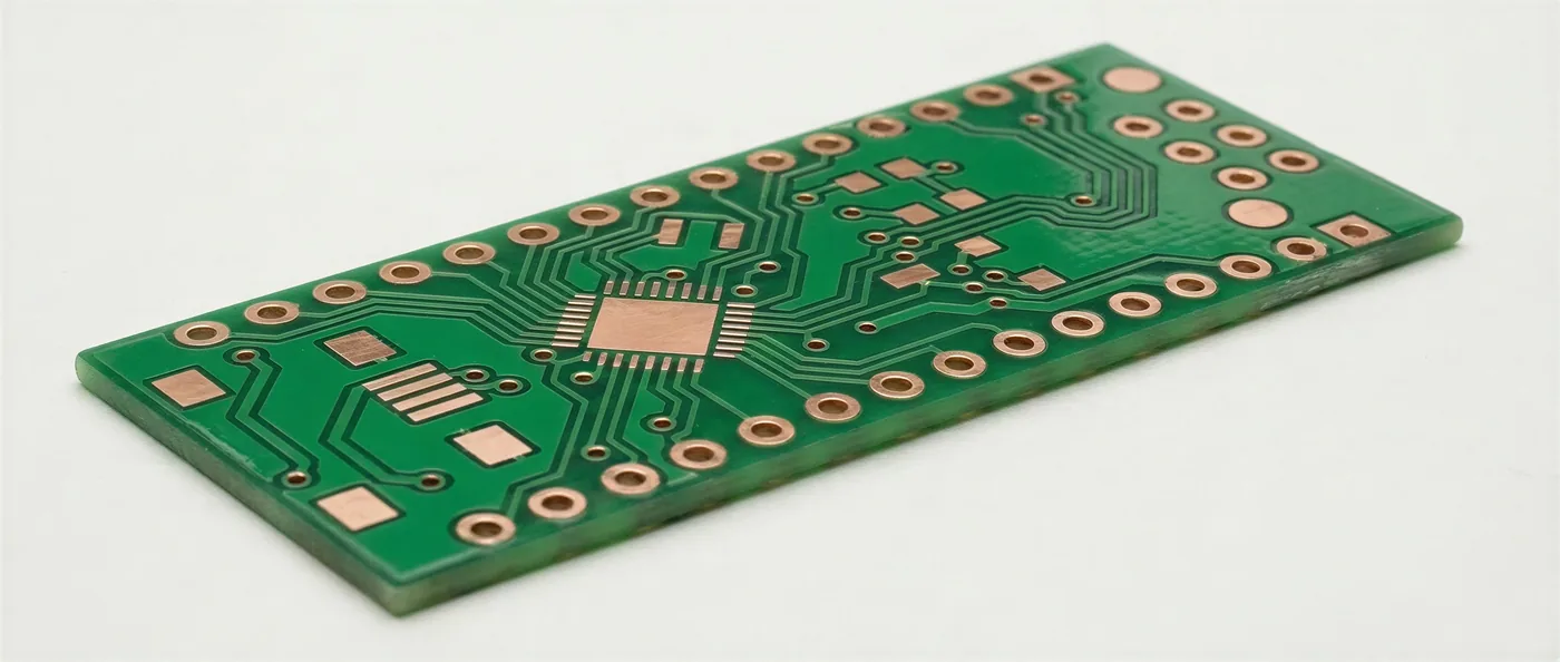
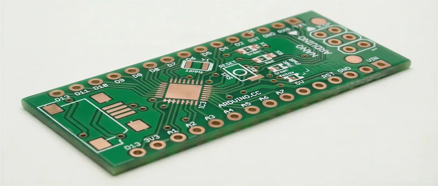
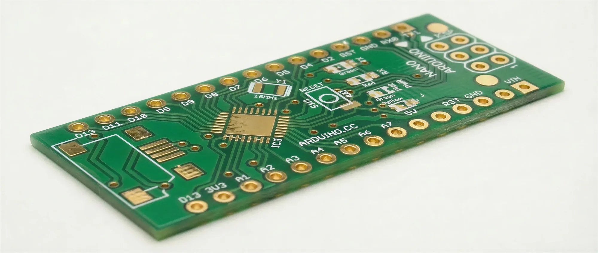
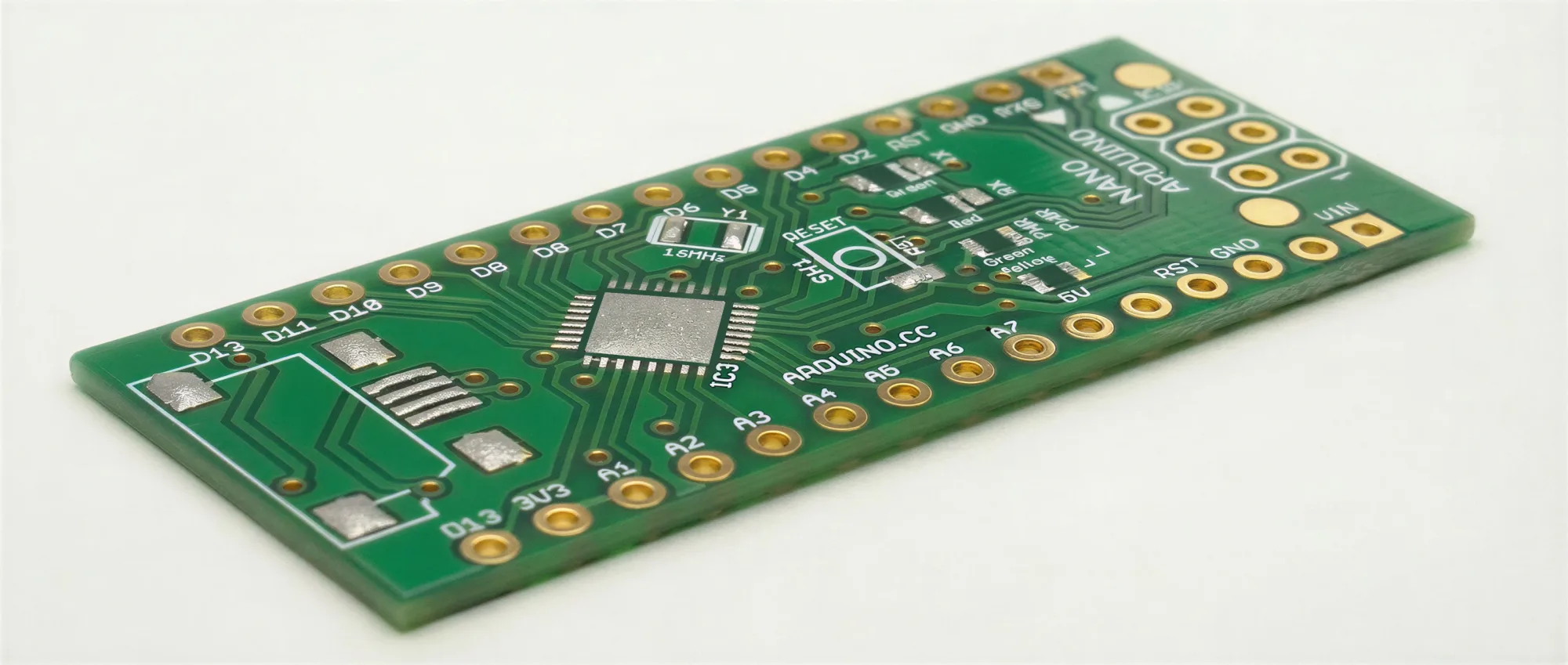
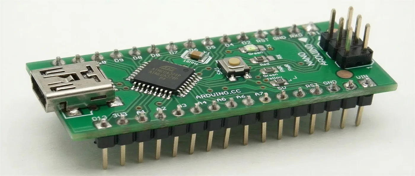
Starting with industry-standard copper-clad FR4 — single- or double-layer substrates.
Two-layer boards are flipped and processed on both sides automatically. The sequence above shows a single-side pass for clarity.
CircuitBuild software
CircuitBuild is the application that turns the CircuitJet IV into a single, coherent machine. It ingests open-standard PCB files, panelizes for the build area, and orchestrates the full inkjet, laser, and SMT sequence.
Because CircuitBuild knows the machine's actual capabilities (trace width minimums, via diameters, throughput, paste deposition tolerances), every job is pre-validated before the laser touches the substrate.
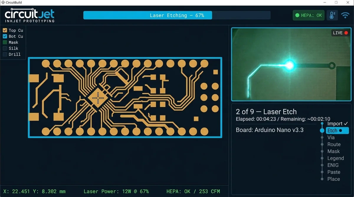
Drag in a Gerber RS-274X or ODB++ file. CircuitBuild auto-panelizes, adds fiducials and tooling strips, and prepares the job for the machine.
Gerber · ODB++ · Auto-panelize · DRC
CircuitBuild runs locally on the machine. No internet connection required. No cloud. No design files leaving your bench. Bottom-vision-verified placement recovery handles drop / mis-pick events without phoning home.
Local · No cloud · No vendor lock-in
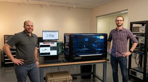
SBIR Phase II · AFX245-PCSO1 · April 2026
The Electroninks team successfully demonstrated CircuitJet IV with the 58th Maintenance Group at Kirtland Air Force Base, under the Air Force Rapid Sustainment Office's Phase II SBIR program.
For commercial teams, the same air-gapped, all-in-one workflow compresses fabrication cycles from weeks to hours.
Technical specifications
* Future add-on extends to 2+ layers.
Join the waitlist
Get on the waitlist for pricing and early-access updates.
We'll email you a confirmation shortly. When CircuitJet IV is ready to ship, you'll be the first to know.
By

CircuitJet IV is a product of Electroninks, the Austin-based materials company behind the particle-free conductive inks used at every major defense prime and semiconductor fab. Our inks are why CircuitJet IV can print a real board. Our balance sheet is why it will ship. And our prior generation, CircuitJet I, is what proved the model.
Air Force SBIR Phase II
Electroninks was awarded a $1.25M Phase II SBIR (AFX245-PCSO1) by the U.S. Air Force Rapid Sustainment Office to deliver on-demand printed-circuit manufacturing to austere environments, powered by the same particle-free conductive inks and CircuitJet IV printing hardware you see here.
Read the releaseStrategic partners
We're hiring · Austin, TX
Architect the gantries, motion systems, and multi-process integration that make CircuitJet IV. Laser, inkjet, paste, and pick-and-place — all on one bench-top platform.
Questions